Overview
Enterprise prototyping is an emerging market that blends emulation with traditional prototyping to provide a solution with enhanced debuggability, high capacity and performance, and the ability to interact with a wide range of peripherals and stimulus.
AMD offers significant advantages for developing emulation and enterprise prototyping platforms including fast place-and-route to improve productivity for large ASIC and ASSP designs, full visibility debug solutions, reduced system-level power consumption, and high utilization and QoR supporting ASIC-like clocking and routing structures.
AMD Vivado ML implementation tools
- Reduced compile time
- Improved QoR
- ASIC-like clocking efficiently maps complex ASIC and SoC clock trees
High bandwidth and low-latency I/O and transceivers
- Efficient pin multiplexing between FPGAs
- Reduced latency across partitions for improved system performance
- Industry support with our High-Speed Transceiver Pin Multiplexing IP
Full Visibility Debug Solutions
- Re-entrant debug probe modifications for quick debug turnaround
- Full debug visibility supporting configuration-based readback, writeback, and state capture
- High-speed debug over PCIe® and deep storage ILA to offload capture data to external memory
Portfolio

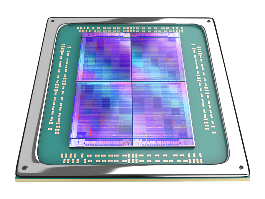
AMD Versal™ Premium VP1902 Device: World’s Largest Adaptive SoC4
The AMD Versal™ Premium VP1902 adaptive SoC is the first emulation-class device to feature a scalar processing subsystem on-chip, which enables a wide range of control and stimulus generation use modes for SW/HW firmware development and system bring-up.
The VP1902 device doubles device capacity2 compared to the Virtex™ UltraScale+™ VU19P device in order to fit larger IP and design subsystems. The on-chip A72 Arm® processor enables a wide variety of prototyping use cases for software and hardware co-development. Our XPIO and MIPI D-PHY enable a wide variety of at-speed peripheral stimulus. These silicon features combine to provide an ideal solution for tackling the prototyping demands of cutting-edge ASIC, IP, and SoC development.
Featured AMD Adaptive Computing Partners
Get Started
Prototype with AMD Versal Premium
AMD Versal™ Premium VP1902 Device: World’s Largest Adaptive SoC
- 2X higher logic density2 compared to the AMD Virtex™ UltraScale+™ VU19P device
- 2X aggregate I/O bandwidth5 and 2.3X transceiver bandwidth6 for scalability
- Reduced I/O latency and two-by-two SLR array for improved system performance
AMD VivadoTM ML Design Suite
The AMD Vivado™ ML design suite delivers a state-of-the-art development experience with new implementation features designed to improve compile time and QoR.
Support & Resources

Contact Sales
Our sales team is here to support you in making the best technology decisions based on your specific needs.
Footnotes
- Based on AMD internal analysis, May 2023. (VER-009)
- Based on AMD internal analysis in May 2023, comparing the number of system logic cells of the Versal Premium VP1902 device versus the Virtex UltraScale+ VU19P device. (VER-001)
- Based on AMD internal system clock performance analysis in May 2023, comparing the Versal Premium VP1902 device to the Virtex UltraScale+ VU19P device across a range of design sizes and cut nets. (VER-006)
- Based on AMD internal analysis in May 2023 with a 6-input LUT count to compare the Versal Premium VP1902 device versus the Intel Stratix 10 GX 10M FPGA. (VER-002)
- Based on AMD Labs testing using an A6865 package to simulate the XPIO data rate performance of an AMD Versal Premium VP1902 device versus the published data rate of an AMD Virtex UltraScale+ VU19P FPGA. Actual results will vary. (VER-003)
- Based on AMD Labs calculation in May 2023 of aggregate transceiver bandwidth of a Versal Premium VP1902 device B6865 package versus a Virtex UltraScale+ VU19P device B3824 package, assuming GTY/GTYPs running at 32G and GTMs running at 56G. (VER-005)


