矩阵核心技术
AMD CDNA 3 采用矩阵核心技术,具有增强的计算吞吐量和改进的指令级并行能力,支持各种精度(INT8、FP8、BF16、FP16、TF32、FP32 和 FP64)以及稀疏矩阵数据(即稀疏性)。
HBM 内存、缓存和一致性
AMD Instinct 加速器的部分产品具有先进的 HBM3 容量和内存带宽,以及共享内存和 AMD Infinity Cache(共享最后一级缓存),无需数据复制并改善延迟。


统一结构
新一代 AMD Infinity 架构与 AMD Infinity Fabric 技术相结合,可在单器件和多器件平台中实现 AMD GPU 和 CPU 小芯片技术与堆叠式 HBM3 内存间连贯、高吞吐量的统一。它还提供兼容 PCIe® 5 的增强型 I/O。

AMD CDNA 2
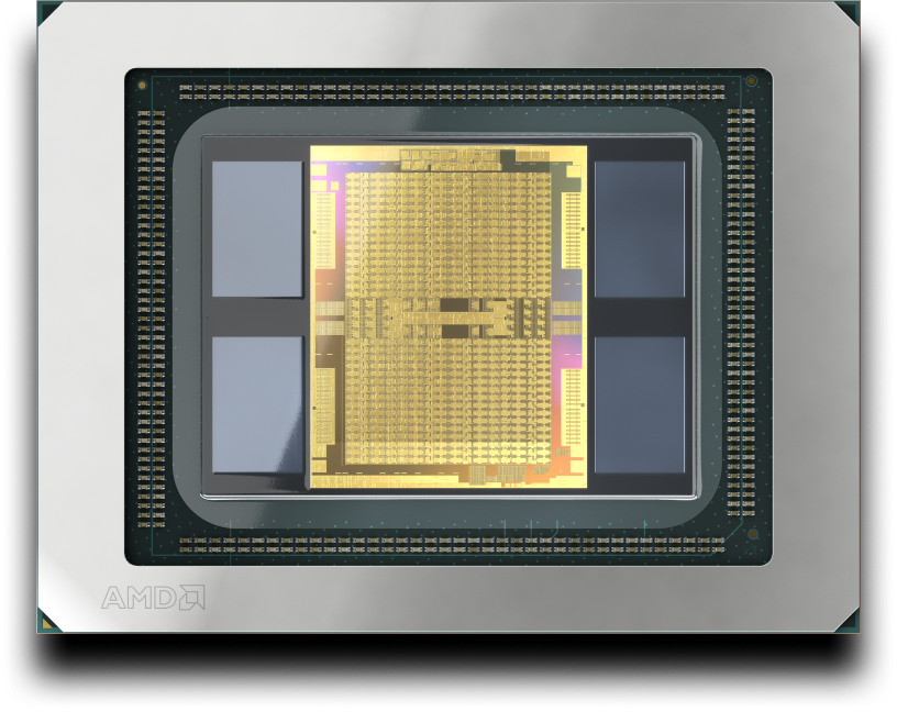
AMD CDNA 2 架构旨在加速极其繁重的科学计算工作负载和机器学习应用。它是 AMD Instinct MI200 系列加速器的基础。

AMD CDNA
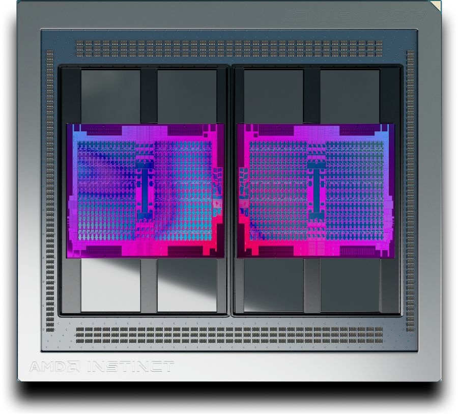
AMD CDNA 架构是一种基于 GPU 的计算专用架构,旨在开创百万兆次级计算时代。它是 AMD Instinct MI100 系列加速器的基础。

AMD Instinct 加速器
了解 AMD Instinct 加速器如何增强 AI 和 HPC 的性能。
附注
©2023 Advanced Micro Devices, Inc. all rights reserved. AMD, the AMD arrow, AMD Instinct, AMD CDNA, Infinity Fabric, ROCm, and combinations thereof, are trademarks of Advanced Micro Devices, Inc. PCIe is a registered trademark of PCI-SIG Corporation. Other names are for informational purposes only and may be trademarks of their respective owners.
- Calculations conducted by AMD Performance Labs as of November 7, 2023, for the AMD Instinct™ MI300A APU accelerator 760W (128 GB HBM3) designed with AMD CDNA™ 3 5nm FinFet process technology resulted in 128 GB HBM3 memory capacity and 5.325 TFLOPS peak theoretical memory bandwidth performance. MI300A memory bus interface is 8,192 (1024 bits x 8 die) and memory data rate is 5.2 Gbps for total peak memory bandwidth of 5.325 TB/s (8,192 bits memory bus interface * 5.2 Gbps memory data rate/8). The highest published results on the NVidia Hopper H200 (141GB) SXM GPU accelerator resulted in 141GB HBM3e memory capacity and 4.8 TB/s GPU memory bandwidth performance. https://nvdam.widen.net/s/nb5zzzsjdf/hpc-datasheet-sc23-h200-datasheet-3002446 The highest published results on the NVidia Hopper H100 (80GB) SXM GPU accelerator resulted in 80GB HBM3 memory capacity and 3.35 TB/s GPU memory bandwidth performance. https://resources.nvidia.com/en-us-tensor-core/nvidia-tensor-core-gpu-datasheet Server manufacturers may vary configuration offerings yielding different results. MI300-12
- Calculations conducted by AMD Performance Labs as of November 17, 2023, for the AMD Instinct™ MI300X OAM accelerator 750W (192 GB HBM3) designed with AMD CDNA™ 3 5nm FinFet process technology resulted in 192 GB HBM3 memory capacity and 5.325 TFLOPS peak theoretical memory bandwidth performance. MI300X memory bus interface is 8,192 and memory data rate is 5.2 Gbps for total peak memory bandwidth of 5.325 TB/s (8,192 bits memory bus interface * 5.2 Gbps memory data rate/8). The highest published results on the NVidia Hopper H200 (141GB) SXM GPU accelerator resulted in 141GB HBM3e memory capacity and 4.8 TB/s GPU memory bandwidth performance. https://nvdam.widen.net/s/nb5zzzsjdf/hpc-datasheet-sc23-h200-datasheet-3002446 The highest published results on the NVidia Hopper H100 (80GB) SXM5 GPU accelerator resulted in 80GB HBM3 memory capacity and 3.35 TB/s GPU memory bandwidth performance. https://resources.nvidia.com/en-us-tensor-core/nvidia-tensor-core-gpu-datasheet. MI300-05A


